
Laser Applications for Semiconductor Manufacturing
Semiconductor manufacturing requires precision, repeatability, and traceability at every stage. UV laser technology delivers permanent, high-contrast marking and precision processing with micron-level accuracy, minimizing contamination, mechanical stress, and thermal damage.
UV laser systems help manufacturers enhance traceability, improve quality control, and support reliable, high-volume production through precise, non-contact processing.
Laser Marking for Wafer Traceability
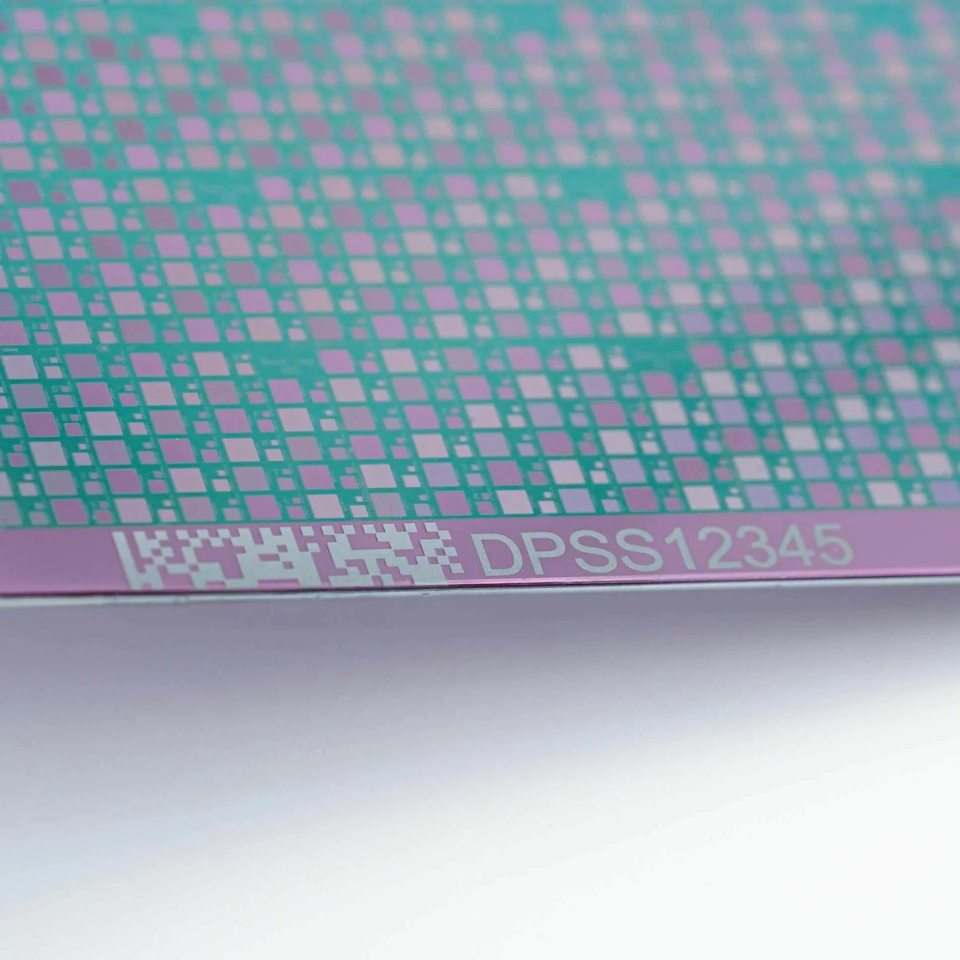
Wafer laser marking provides permanent, high-precision identification for complete traceability in semiconductor manufacturing. It enables precise marking of lot numbers, serial numbers, and Data Matrix codes with minimal surface impact.
Advanced soft-marking techniques reduce debris and contamination risks while delivering repeatable, micron-level accuracy. The non-contact process integrates easily into automated production and downstream processes.
Laser Micro-Texturing for Wafer Surface Engineering
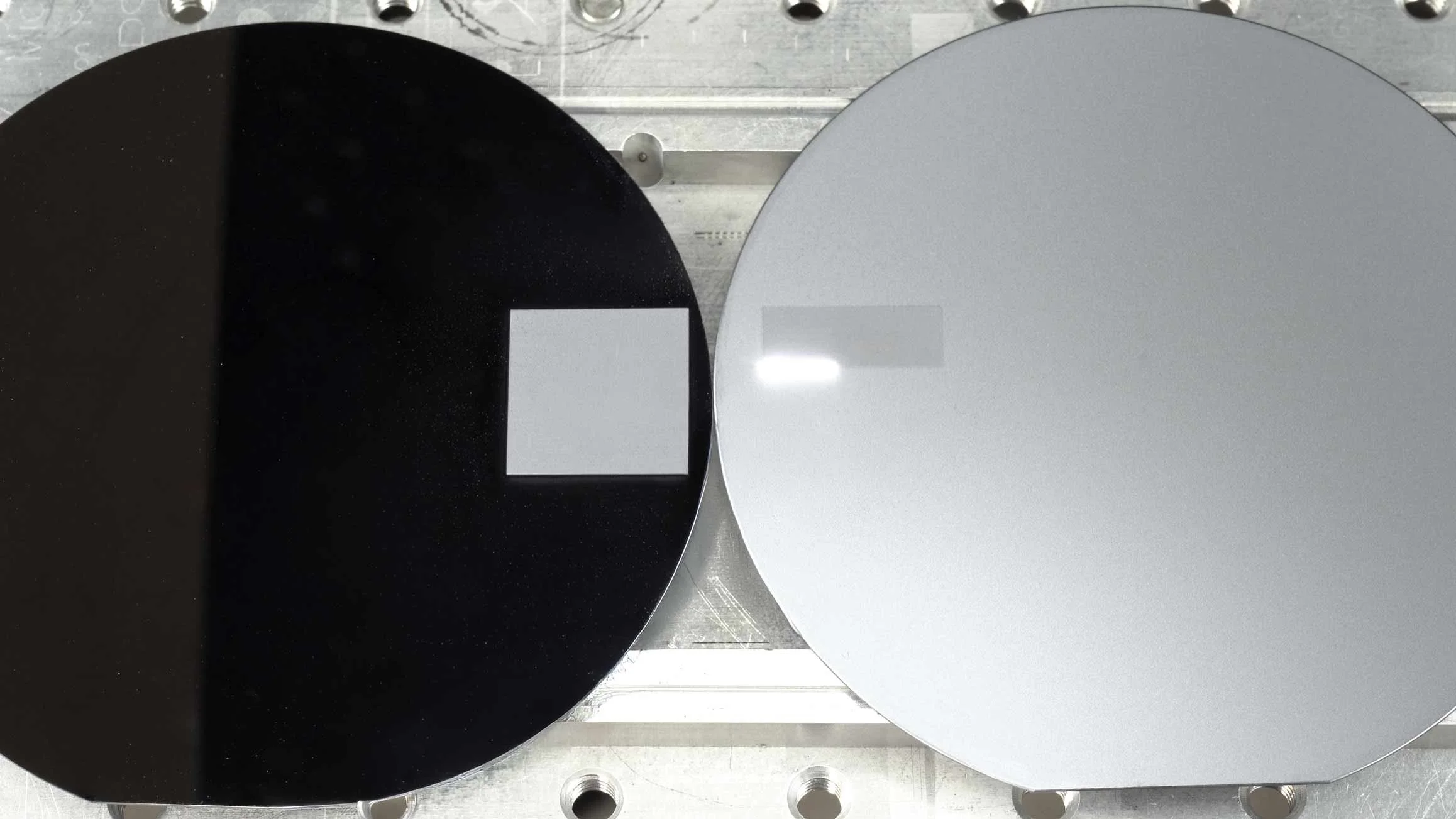
Wafer micro-texturing creates precise surface features on semiconductor wafers to enhance performance, improve process control, and support advanced device manufacturing.
Using ultrafast laser pulses, manufacturers can generate highly uniform microstructures with micron-level accuracy while minimizing thermal effects on the surrounding material. These engineered textures can optimize surface properties such as adhesion, wettability, light absorption, or bonding performance, depending on the application requirements.
Laser Scribing for Wafer Dicing Preparation
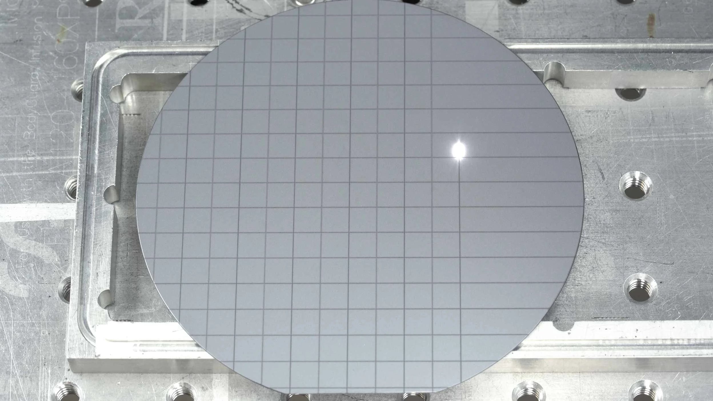
Laser wafer scribing creates precise, controlled fracture lines on silicon and compound semiconductor wafers, preparing them for clean, high-yield die separation.
This process can scribe narrow, shallow grooves along the wafer's crystal planes with micron-level accuracy and minimal mechanical stress. This non-contact process reduces microcracking and edge damage compared to traditional saw dicing, helping preserve die strength while supporting narrower street widths and higher material yield.
Laser wafer scribing is ideal for wafers as thinness and tight die spacing make conventional mechanical dicing impractical.
Laser Cleaning for Wafer Surface Preparation and Reclamation
Laser cleaning removes organics, oxides, residues, and other contaminants from wafer surfaces without damaging the underlying substrate.
This process can ablate unwanted surface layers with micron-level selectivity, leaving the wafer material intact. This dry, non-contact process eliminates the need for chemical baths or abrasive treatments, reducing the risk of substrate damage while supporting cleaner, more consistent surface conditions ahead of subsequent processing steps.
Laser cleaning is well-suited for surface preparation and wafer reclamation, where restoring a contaminant-free, defect-free surface is essential for reuse or continued fabrication.
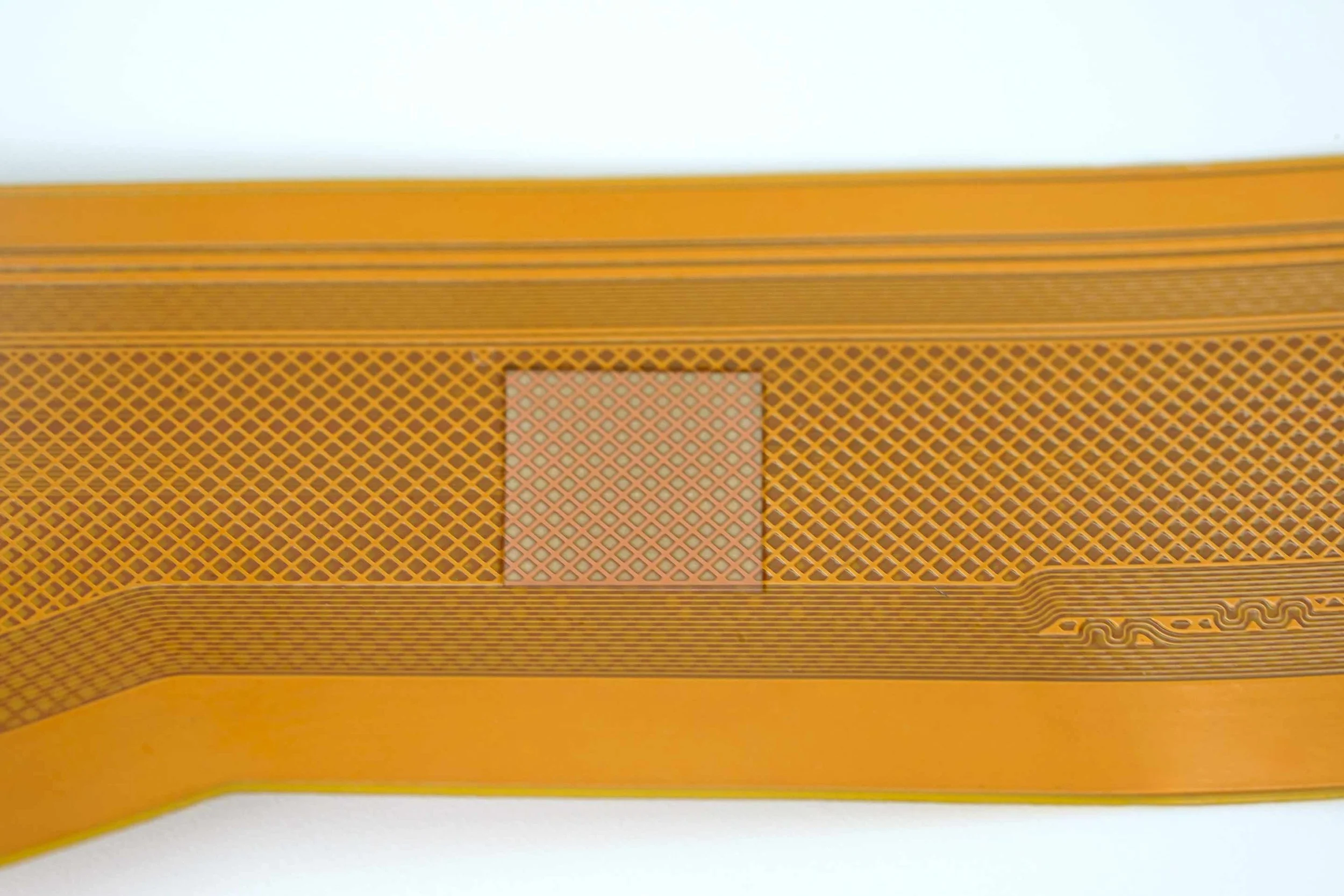
Laser Depaneling of Semiconductor PCBs
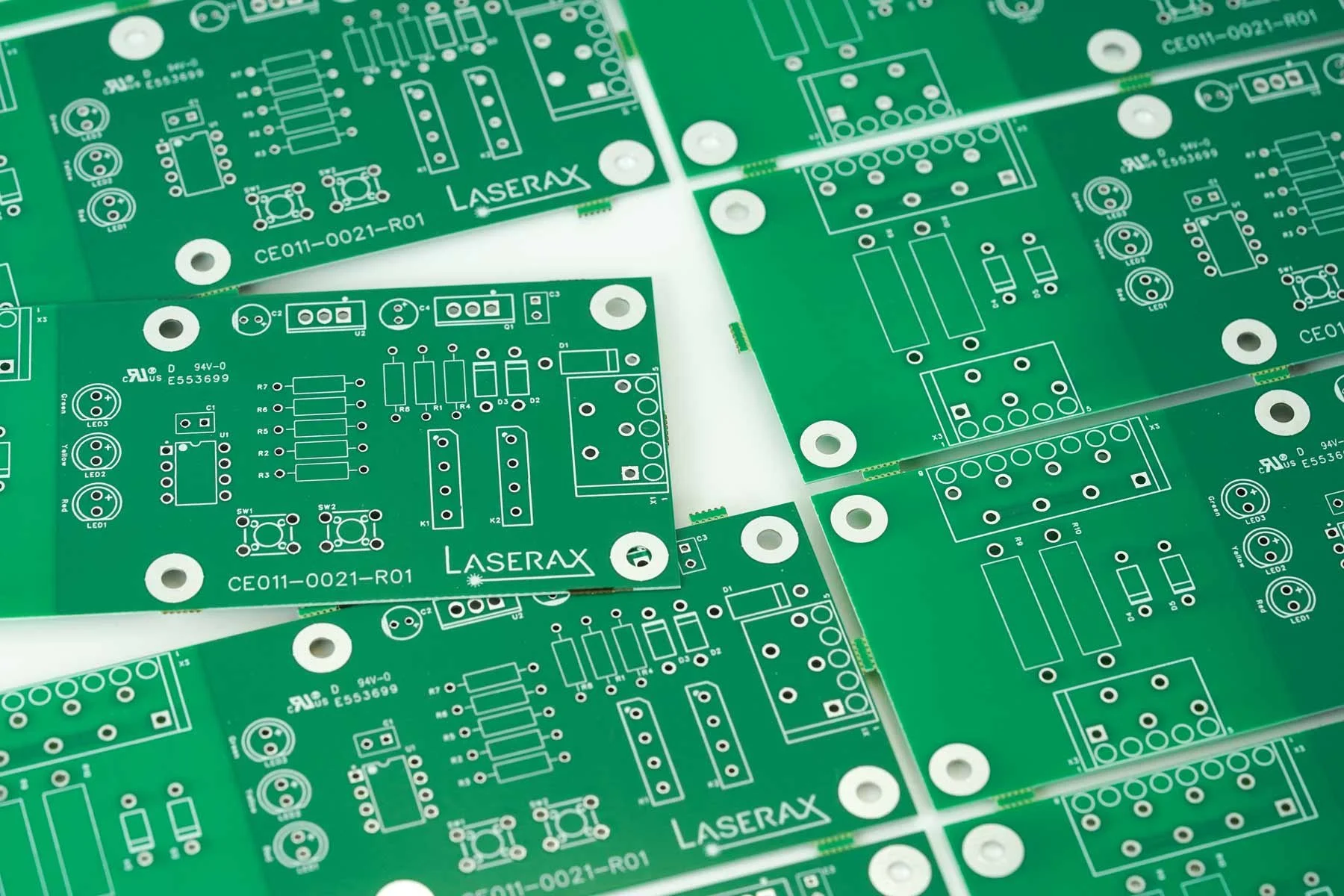
UV lasers enable high-precision PCB depaneling by separating individual boards from a panel without mechanical contact.
Their short wavelength and low thermal impact help minimize the heat-affected zone while avoiding the mechanical stress associated with traditional depaneling methods. This makes UV lasers particularly well-suited for thin, densely populated, rigid-flex, and other sensitive PCB assemblies. As a result, manufacturers can achieve clean-cut edges, protect nearby components and circuits, improve yields, and support increasingly compact PCB designs.
Laser Technology Benefits For Semiconductor Manufacturing

Non-contact process for delicate components
Laser systems mark wafers and semiconductor packages without physical contact, eliminating the risk of mechanical stress, cracking, or surface contamination.

Micron-level precision with minimal heat impact
Advanced laser technologies produce extremely fine marks with controlled energy input, minimizing heat-affected zones and preserving wafer integrity.
Permanent traceability throughout production
High-resolution serial numbers, Data Matrix codes, and lot identifiers remain readable throughout manufacturing, ensuring traceability from fabrication to final assembly.

Seamless integration into automated production lines
Laser marking systems integrate easily with robotics, machine vision, MES platforms, and inline inspection systems, supporting high-throughput semiconductor production and automated quality control.